I finally got SCSI working on my X68030 CZ-500C, so thought I’d do a writeup on what I learned. It will be in two parts, where the first one covers the default CZ-500C SCSI support, and the second part covers a new adapter I made for using internal SCSI devices.
CZ-500C SCSI Internals
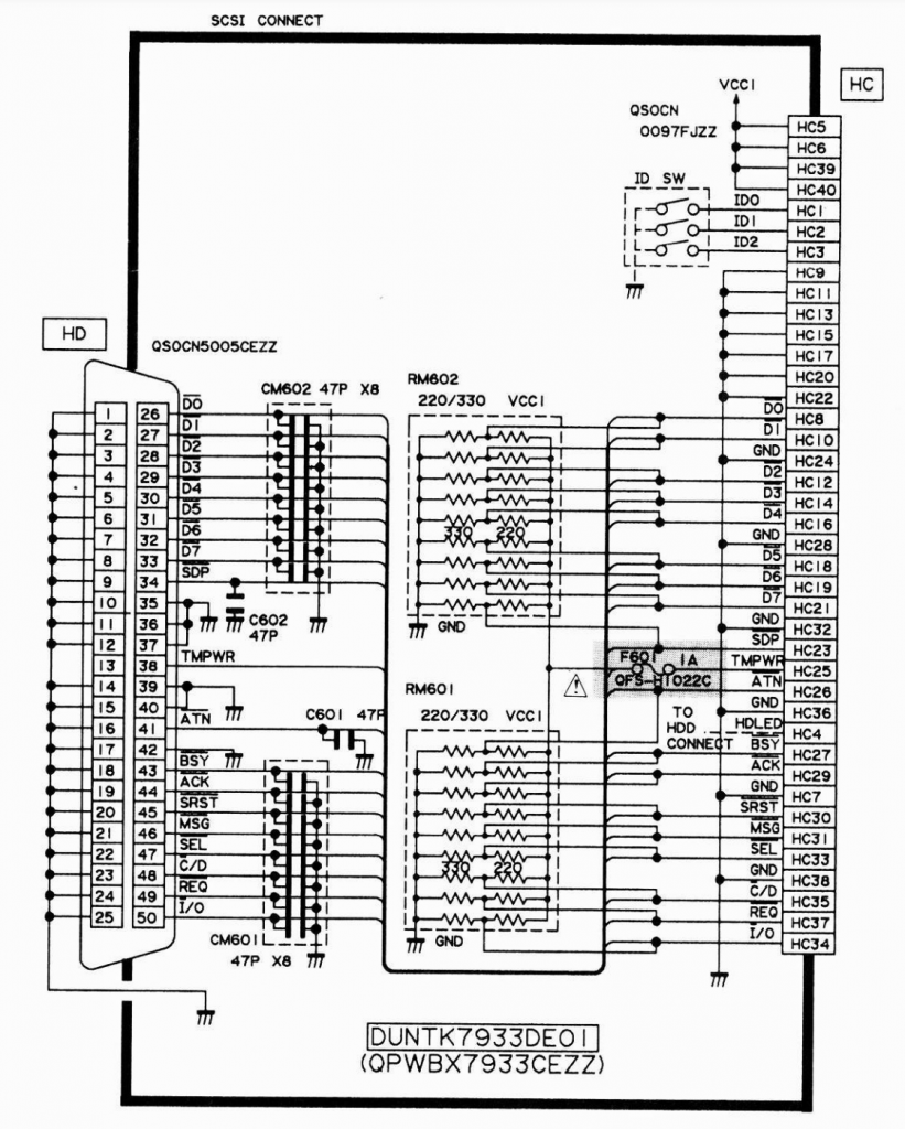
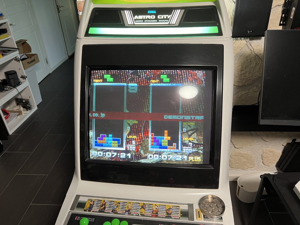
X68030 has proper SCSI support, not just SASI as some of the earlier X68000 models. CZ-500C does however lack cabling for internal SCSI HDD (which CZ-510C has). The internal connector used from the main board to the SCSI IO board is a non-standard 40-pin flat cable. The schematic for CZ-500C including the SCSI board can be found here.
The IO board itself is quite simple. Other than the connectors and ID switch, it just has a terminating 33oΩ/220Ω resistor network, a bunch of capacitors and a 1A fuse for the external power delivery. It is mounted on top of another IO board for the external floppy, and easy to remove with two screws.
If the SCSI board is not connected to the bottom PCB of the X68030, the system will not start.
External connectors
The external SCSI connector is a “Micro Centronics” connector, which is hard to find proper cabling for. It seems like the Japanese term for these are アンフェノールハーフ50 (Amphenol half 50) or アンフェノールハーフピッチ50 (Amphenol half pitch 50).
When looking for adapters to full-size Centronics, you can search for that in combination with アンフェノールフル 50 (Amphenol full 50), and look for a cable with a male Micro connector that goes to a female full size connector. This can then be hooked up to a Centronics Bluescsi device. Example from an Mercari auction:
There is a SCSI ID switch on the back of the unit. This doesn’t seem to be related to the external device, but rather the SCSI ID that the X68030 uses. Weirdly there’s also an option for this in SWITCH.X so I’m not really sure which option has priority. The compact version of X68030 does not have this switch, nor does other X68000 models as far as I can tell.
Did a quick recap of my new PC-9801-86, and thought I’d add some notes to simplify for other people. There’s an earlier Japanese caplist here that I used as a base, but they used THT caps for the recap which I didn’t want to do.
Note that C33 and C34 are bipolar caps. The mouser links below link to the proper ones, but in my actual recap I just used polarized capacitors which seems to work as well (the Japanese link above did this too). It should be better to use bipolar caps though, so I might swap them later.
This is honestly the only tricky part, and the main thing is that the disk images are incompatible with greaseweazle as far as I can tell, so first you need to open Virtual Floppy Image Converter and convert it to a FM Towns compatible format.
Select “D88 format” as format and click the open icon to the left
Select FDMINI.BIN
This will then spit out a D88 image.
Connect your Greaseweazle over USB. Hook up the 3.5″ floppy drive to it. Use a twisted floppy cable. Run:
gw write fdimage.d88 --drive=A
This will produce the floppy you need
Booting
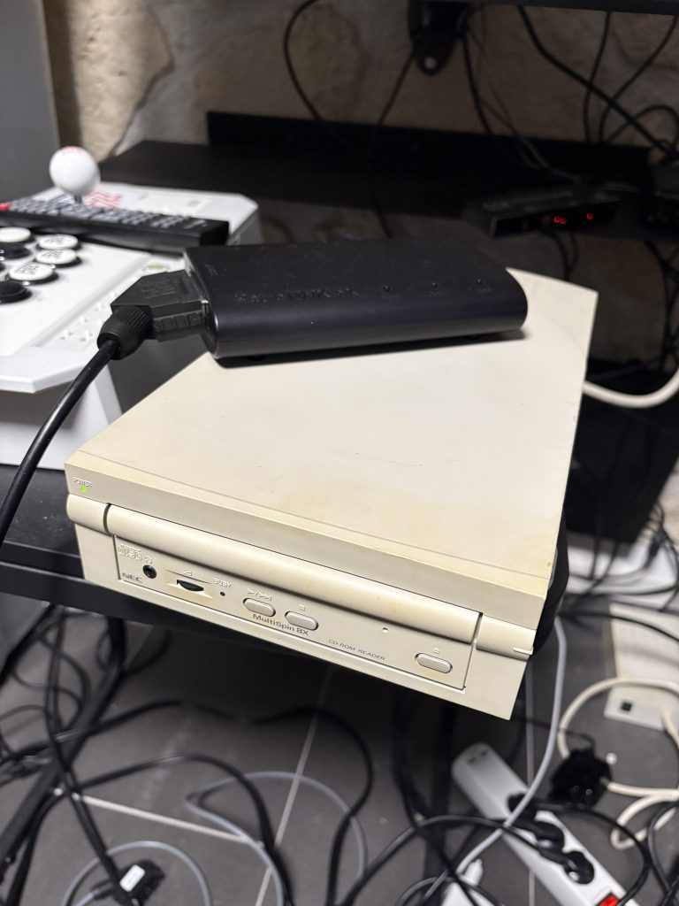
Connect the SCSI CD-ROM drive to the SCSI port at the back of the FM Towns and put a CD in it. Use the boot floppy and it will automatically boot from the external CD-ROM.
For quite a while now, I’ve known that converting Ibara PCB’s to Ibara Black Label without any soldering is possible with a minor audible difference. The character select music from Ibara Kuro is not present on the regular Ibara roms, which is not solvable without re-soldering.
Other than that, the music roms are identical, and since both the U2 and U4 roms can be reprogrammed through JTAG, that means that a conversion between them is possible, although it will be be noticable on the character select screen.
This post covers that a bit more in-depth.
Difference in music ROMs
If running the Audio_ExtractData scripts in my cv1k research repo on the Ibara and Ibara Black Label romset and then comparing checksums, it becomes clear that every entry in the list of sounds match except the first two.
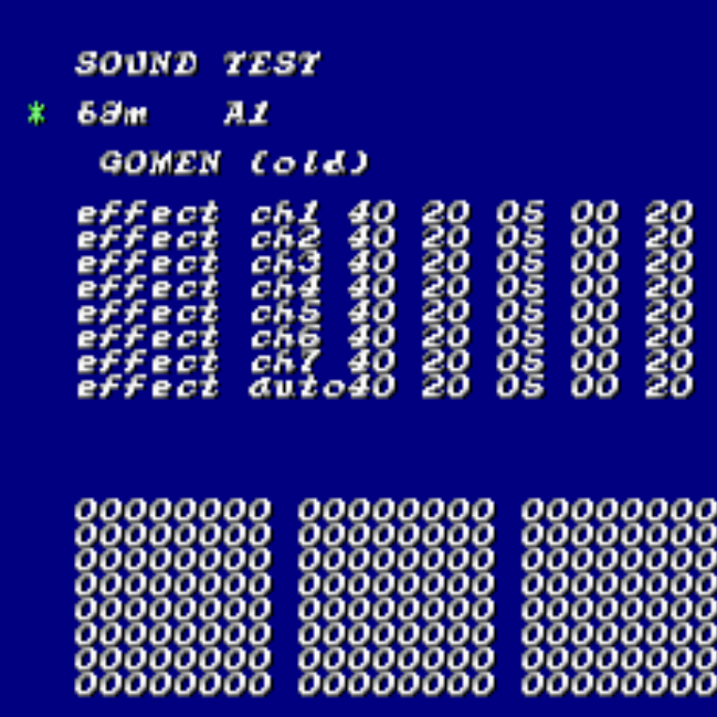
On the regular Ibara sound ROMs, this seems to be some unused placeholder music from Mushihimesama. If inspecting the name for these in the program data, there’s some strings such as “GOMEN (old)”, which can also be checked in the test menu through memory hacking. Playing these will play some of the Mushihimesama music.
The track at ID=0 is just about a second, but the one at ID=1 is about 28 seconds long.
If inspecting the music in the first two slots of Ibara Kuro, then one can notice that the first one holds the new Character Select music, which is the only new tune (about 47 seconds long).
This means that simply swapping the non-music roms on the board would have the character select music play a second of Mushihimesama music, and then silence… which isn’t the end of the world, but we can improve that slightly!
Modifying the Ibara Kuro U4 rom to play nice with character select music
The simplest thing to do here is to swap the track played on character select screen. After reverse engineering the program code, the TL;DR is that this is controlled by the byte at offset 0xC186F of the Ibara Kuro U4.
By default it’s set to 0x00 which would play a second of Mushihimesama music. Changing it to 0x01 will have it play the longer Mushi tune, which I felt was sufficient. Changing it to 0x10 will have it play “Showtime” which was the original Stage 1 music that was not used in Ibara Kuro for some reason, so that’s also a good option.
TL;DR: Change the byte at 0xC186F from 0x00 to 0x01.
Then with the U4 modified for the character select screen:
# This will take a few hours with UsbBlaster, and less than
# an hour with Tigard
sudo jtag
jtag> cable UsbBlaster
jtag> detect
jtag> detectflash 0
jtag> flashmem 0 u4.bin
Writing U2
It’s VERY VERY IMPORTANT to make a backup of the initial block of your PCB first. CV1000 programs around initial bad blocks of the NAND, and if you lose your bad block table, than that can lead to bad behavior later.
# Store this somewhere safe
sudo python3 K9F1G08U0M_JTAG.py read_page --page=0 --filename=u2_page0.dump

# Then run this to print the bad blocks
sudo python3 K9F1G08U0M_JTAG.py bad_blocks
Honestly, probably not. The base game plays better, and Black Label feels a bit like a weird romhack. Unless you are confident messing around with expensive hardware, I’d avoid doing it. The setup is somewhat complex.
If you however end up doing it, make extra sure to backup your bad block table and don’t complain to me if you break something.
But yeah, if you have several Ibara boards and you know what you are doing, then this can be fun to do on one of them since you can always reverse it later 🙂
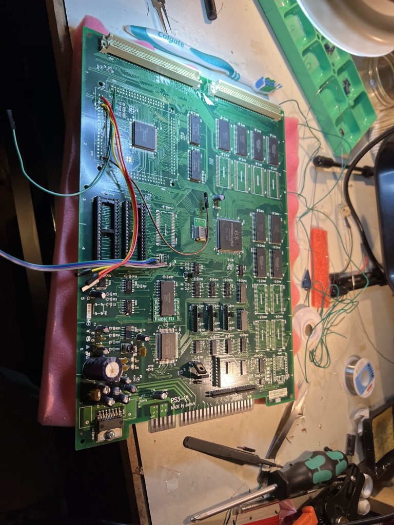
… which is really nice, because I own most of the early Psikyo games, but on this hardware I only had the original PCBs for Strikers II, Gunbird 2 and G-Taste (best jong game).
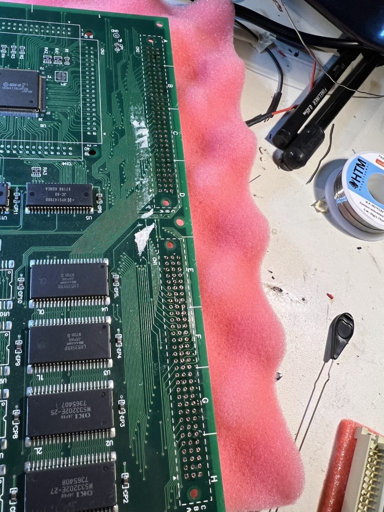
Went ahead and converted my Strikers II which was… not too bad! Clearing the holes for the adapters of the sub-pcb was a bit of work, but with a good desoldering station it was fine.
With an inspection microscope, the rest of the install was pretty simple.
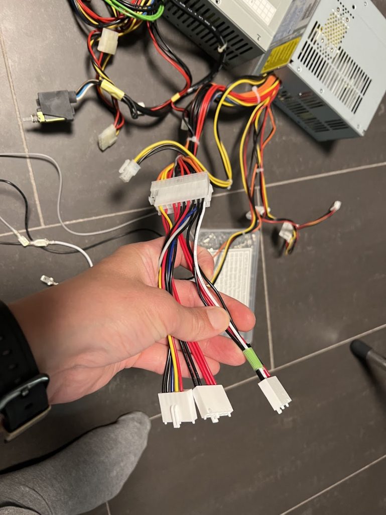
The PSU is the same size as standard “small” ATX power supplies, which is 150mm (W) x 86mm (H) x 140mm(D). For the replacement PSU, make sure to find something with suitable power placement to fit the holes in the case. Modern PSU’s will usually have different fan placement, so you might have to track down some older ones.
The V13 uses standard AT for the main two connectors except:
-5V is not populated
PG (power god) is not populated
This means that the cabling is as follows:
Black = GND
Green = 3.3V
Red = 5V
Yellow = 12V
Blue = -12V
I simply grabbed two AT->ATX power adapters and moved one of the AT cablings to free slots for 3.3V and GND in the ATX adapter. One GND pin is unpopulated, but that should be fine (and does seem to work well).
The (probably nicer) alternative is to simply remove the cabling from the original AT power supply and crimp ATX pins on those, to get the colors completely right too.
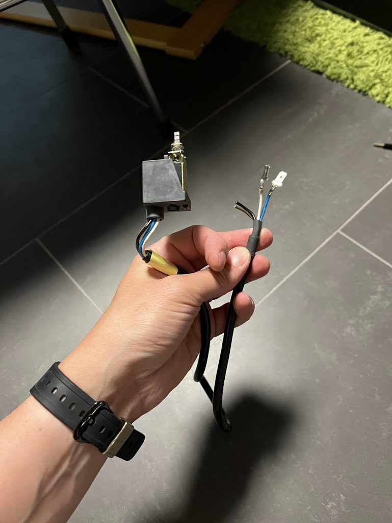
For power, rip out the original AT powr wiring and hook up the blue and white wires to PS_ON and GND on ATX. This will make the PSU work similar to the original one.
Did a full recap on my V13 PC-9821. Here is the cap list. I did double check the values, but there’s still a possibility for errors, so I recommend checking them yourself too.
Motherboard
1A2: 100u, 16v (6.5mm)
1A9: 100u, 16v (6.5mm)
1A10: 47u, 16v (5mm)
1B13: 10u, 16v (5mm)
1H1: 10u, 16v (5mm)
1H2: 10u, 16v (5mm)
1H3: 47u, 16v (5mm)
1H4: 10u, 16v (5mm)
1H5: 10u, 16v (5mm)
1J3: 47u, 16v (5mm)
1J5: 47u, 16v (5mm)
1J6: 10u, 16v (5mm)
2B5: 47u, 16v (5mm)
2E1: 47u, 16v (5mm)
2H7: 47u, 16v (5mm)
2K3: 47u, 16v (5mm)
3C5: 47u, 16v (5mm)
3D1: 47u, 16v (5mm)
3E11: 10u, 16v (5mm)
3E12: 10u, 16v (5mm)
5B1: 3300u, 10v (12.5mm)
5B2: 47u, 16v (5mm)
5C2: 47u, 16v (5mm)
5M6: 47u, 16v (5mm)
6F3: 10u, 16v (5mm)
6N7: 10u, 16v (5mm)
7F8: 10u, 16v (5mm)
7J7: 10u, 16v (5mm)
7K6: 10u, 16v (5mm)
8G1: 47u, 16v (5mm)
8J1: 10u, 16v (5mm)
9D2: 47u, 16v (5mm)
9D3: 10u, 16v (5mm)
9E3: 10u, 16v (5mm)
9F9: 10u, 16v (5mm)
9G1: 10u, 16v (5mm)
10B2: 47u, 16v (5mm)
10D2: 47u, 16v (5mm)
10F1: 47u, 16v (5mm)
10G1: 10u, 16v (5mm)
10K1: 10u, 16v (5mm)
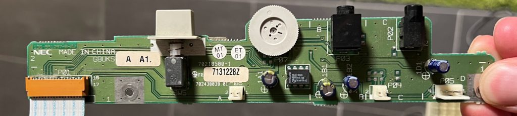
Front IO Board
1A1: 100U, 16V (6.5mm)
1B1: 100U, 16V (6.5mm)
1B2: 10u, 16V (5mm)
1D1: 10u, 16V (5mm)
CBUS Riser
C1: 10u, 16V (5mm)
C2, C3: Unpopulated
C4: 47u, 16V (5mm)
C5: 10u, 16V (5mm)
C6: 10u, 16V (5mm)
C7: 10u, 16V (5mm)
C8: 47u, 16V (5mm)
The slots are 100 Pin 2×50 Edge connectors. 5mm between pin rows. Pin rows have 2.54mm spacing
Sound board
Component markings are super confusing here, but it has
I have dumped a fair amount of arcade ROMs for preservation purposes (a few notable examples being alternative revisions of Batsugun and Dogyuun, as well as several Namco System 10 games), and currently my preferred programmer is a Elnec BeeProg 2C.
This is a nice device, with a big drawback. It’s expensive and the adapters for it are proprietary and very expensive. A single adapter can cost over 200eur and will only be useful for a certain type of IC’s, and this doesn’t just mean the packages type. As an example, TSOP48 NOR and NAND flash will require different adapters.
Easily over 1000EUR in adapters…
Getting one of these if you only want to dump a few ROMs probably won’t make much sense, but if you are an advanced hobbyist, I think throwing money at this problem is well worth it.
So why get this instead of something cheaper?
Simply put, after using different types of cheap Chinese universal programmers I got annoyed enough that I felt the need to upgrade to something that:
Has support for (essentially) all type of chips I’ll want to dump.
Produces reliable dumps that I feel like I can trust.
Writes ROMs reliably with high success rate.
Support writing old CPLD’s with proper vendor algorithms.
Feels like a professional device. Has a known manufacturer with non-suspicious software.
Elnec Beeprog2 checks all these boxes. It’s expensive, but KNOWING that it will produce reliable results is worth the extra spend to me.
One of these is not like the others
… So, what’s so bad about the cheap ones?
Quite a few things really, lets try to break it down into a few sections.
The software
Getting software for the cheap universal programmers means dealing with one of the following:
Needs to be fetched from random electronics forums, because there’s no homepage for the maker of them or any official means to get the software. Sometimes they ship with this software on a CD. Sometimes they won’t.
Can be downloaded from an official webpage that look sketchy as fuck. Hell, TL866II/Xgecu is very popular and their official support is some random QQ email and the software is hosted on mediafire.
It’s not a bad idea to have a separate PC just to use these types of software, cause I have zero faith that they won’t include malware…
… especially since I experienced that myself when I bought a RT809H (don’t ever do this). The software for this device is full of viruses. This is true both for the included CD and from the official website.
If you see this programmer, run away.
Additionally, the UI for the software itself usually looks sort of sketchy, although I will admit the TL866/XGecu software is not too bad, if ignoring the poor translation from Chinese.
Reliability
I’ve had experiences with both incorrect reads and failed writes at a higher rate on the cheaper devices, especially TOP3000. While this can be mostly sidestepped for dumping by reading a ROM several times and making sure that checksums are consistent, it’s not a good feeling.
Failures on burning EPROMs were not uncommon for me with these devices either.
Some devices such as TL866II require manual splitting of larger DIP ROMs, which introduces points of potential failures.
I don’t have high hopes that these devices properly implement the algorithms and settings of more unusual devices, but usually they will kindof work.
Device support
Dumping common ROMs will usually work, but when having to read or write more obscure parts, the cheaper programmers just won’t work at all. For roms this can mean things like TL866II not supporting larger Flash ICs, but I’ve also hit this several times when having to dump devices with internal roms. One recent example is MX10EXA internal rom on “Crazy Bugs”.
Original one + repros. You wont write to these with a cheap programmer.
If you are going to dump and/or build stuff as a hobby, you will keep running into issues like this basically. It is not great.
Ok… but is it a Beeprog worth it though?
I mean… if you have sufficient disposable income to motivate buying one without significantly impacting your personal economy, and want to make sure you have a reliable device that always works then yeah, definitely!
If you just want to burn/dump a few common types of ROMs then probably not.
It’s the same as any other tool really. If you just wanna do some simple cuts of plywood, you don’t need a Festool TS 55 track saw… but if you are going to use it a lot, you are unlikely to regret getting it. For now I’m just renting a TS 55 when I need one, but there is no such option for a Beeprog…
My X68000 (CZ-600C) was failing VRAM checks for Text RAM, and there wasn’t much info available about that online, so I’m writing some up here.
TL;DR information that is good to know:
On CZ-600C, IC1-IC16 is Text VRAM. IC17-IC32 is Graphics VRAM. All 32 of these RAM chips are on the Graphics sub-board.
The RAM IC’s used are MB81461-12 (32 of them).
Addressing for these can be found on the X68000 schematic. This will help narrow down which one is faulty, if you know the bad adresses.
Donor RAM IC’s can be found in Mega Drive units (two per unit).
Debugging the issue
Running MEMTEST (philly 1993) showed this error for TEXT MEMORY.
For more indepth understanding of the errors I ran Memtest68k which showed the range 00e725c – 00e725fc being bad, with Bits in Error Mask: 0000f000.
Looking at the technical guide for X68000 available here , this means that the error is in the last page of Text RAM, and the problematic bits are the highest 4 adresses. Looking at the schematic available on that page, this looked to be either IC16 or IC32 (turns out later it was IC16).
Addressing for Text and Graphics VRAM is slightly different, but the lower numbered IC’s map to the lower address ranges (as expected), and the data bus numbers for the pins in the schematic can help narrow down where the issues is.
To verify if it was IC16, I desoldered pin1 and pin2 on it, and wiggled them a bit while running memory checking. This produced more errors in the page of the already faulty range, which verified that it was indeed this IC that had issues. The main reason for doing this verification was that I was not sure if the first or last 16 RAM chips were for the Text part of VRAM.
After this, I was sure which part was bad.
Fixing the issue
Fixing the issue at this point was pretty straight forward, since it just meant swapping the bad part. Sourcing these are a bit awkward, but there are some available at aliexpress. I didn’t feel like waiting though, so I opened up my Mega Drive and grabbed the video RAM from that, since it uses the same IC’s. I’ll replace that later with the aliexpress ones, whenever they show up.
For desoldering these, you NEED a proper desoldering station/gun. I use a HAKKO FR301-22, but you can use cheaper ones as well. Overall, extracting this type of package is more annoying that DIP packages, but it worked out fine, with not messed up pads.
Removing RAM from Mega Drive
Next step is removing graphics sub-board and RAM chip from the X68000. Then just solder the Mega Drive RAM in the place of the bad RAM.
And there we go, memory test works now! All is good.
There’s is a long-standing belief that MAME has high input lag for Psikyo games (especially earlier titles), so I decided to have a look.
Some people use an ancient MAME-fork called “Shmupmame“, since it has less input lag for these games. I assumed this was due to bugs in the MAME driver, so I started probing some PCBs of mine to figure out how they work.
The MAME drivers report 4 frames of lag on the earlier titles (which is also what I saw when emulating them), and while I did find some things worth adjusting in the MAME driver, these things don’t have any impact on latency. I did however find something else interesting…
Early Psikyo PCBs have quite a bit of lag!
So yeah, the TL;DR is that MAME is accurate, because the Early Psikyo PCBs also have the same amount of input lag. The relevant games are:
Sengoku Ace / Samurai Aces
Gunbird
Battle K-Road
Strikers 1945
Tengai / Sengoku Blade
“Frames of input lag” is a ambiguous term though, so to be clear:
Button/lever is pressed during frame 0
No sprite movement on frame 1
No sprite movement on frame 2
No sprite movement on frame 3
Sprite movement on frame 4!
Also note that when playing original hardware, the input lag will vary by up to one additional frame depending on the raster beam position of the screen at time of button press, since inputs are sampled once per frame. Additionally sprites further up on the screen will be updated quicker, since the beam scans up-to-down.
Here is two typical example of what it can look like on Tengai shot in 240fps.
Note that time from button press until bomb animation starts is the same as for lever input to player movement in this game (in some other games that is not true).
Img 5: Button is pressed right AFTER it gets sampled.
Img 6-8: Game still doesn’t know button was pressed
Img 9: Finally button is sampled
Img 10-13: One frame of no sprite movement
Img 14-17: One frame of no sprite movement
Img 18-21: One frame of no sprite movement
Img 22: Bomb animation starts
Tengai in MAME
In MAME, the easiest way to verify that its similar timing as on PCB is to do the following:
Bind buttons for “Pause” and “Pause – Single Step” (UI input menu)
Pause game while not inputting anything
Hold bomb button (or direction) when paused, and doing steps below
Pause Single Step (One frame of no sprite movement)
Pause Single Step (One frame of no sprite movement)
Pause Single Step (One frame of no sprite movement)
Pause Single Step (Animation starts)
Basically… everything seems fine.
What about later games?
Later games have much lower input latency on PCB. These include:
Sol Divide
Strikers 1945 II
Strikers 1945 III
Gunbird 2
Dragon Blaze
…
… but they do on MAME too.
When testing Strikers 1945 II on PCB, I get one frame of no sprite movement. MAME produces the same result as PCB if using the Pause+Step method described above.
Basically, the newer games have two frames less input lag on both PCB and MAME compared to the older games.
But shmupmame has less lag on the early games right?
Yes, shmupmame has less lag than MAME and original PCBs for early Psikyo games. It does this by shortcuts that are possible since some buffers can be safely skipped in emulation, if not worrying about emulating the hardware accurately. If you prefer to play these games like that, then that’s fine too. It’s just not how the games worked originally 🙂